- 您现在的位置:买卖IC网 > Sheet目录415 > FDB8445 (Fairchild Semiconductor)MOSFET N-CH 40V 70A D2PAK
�� �
�
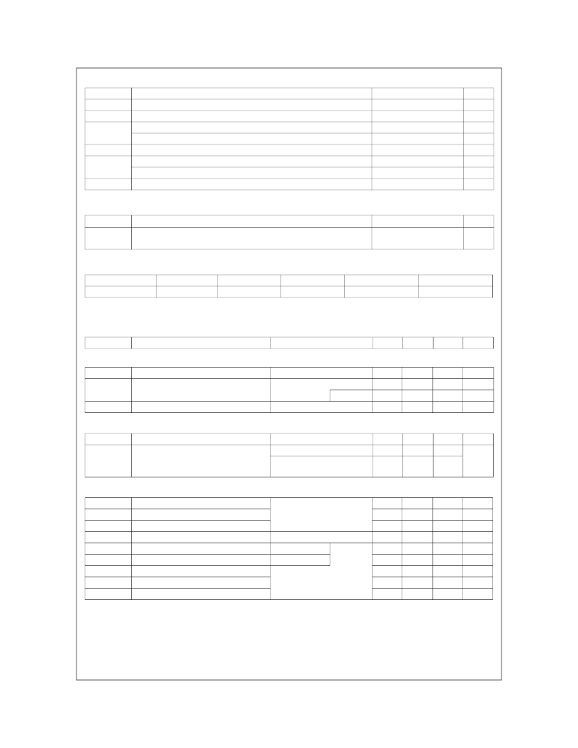
�Absolute� Maximum� Ratings� T� C� =� 25°C� unless� otherwise� noted�
�Symbol�
�V� DSS�
�V� GS�
�Drain� to� Source� Voltage�
�Gate� to� Source� Voltage�
�Parameter�
�Ratings�
�40�
�±20�
�Units�
�V�
�V�
�I� D�
�E� AS�
�P� D�
�Drain� Current� Continuous� (V� GS� =� 10V)�
�Pulsed�
�Single� Pulse� Avalanche� Energy�
�Power� Dissipation�
�Derate� above� 25� o� C�
�(Note� 1)�
�(Note� 2)�
�70�
�Figure� 4�
�102�
�92�
�0.6�
�A�
�mJ�
�W�
�W/� o� C�
�T� J� ,� T� STG�
�Operating� and� Storage� Temperature�
�-55� to� +175�
�o�
�C�
�Thermal� Characteristics�
�R� θ� JC�
�Thermal� Resistance,� Junction� to� Case�
�1.63�
�o� C/W�
�R� θ� JA�
�Thermal� Resistance,� Junction� to� Ambient� TO-263,�
�area�
�1in� 2�
�copper� pad�
�43�
�o� C/W�
�Package� Marking� and� Ordering� Information�
�Device� Marking�
�FDB8445�
�Device�
�FDB8445�
�Package�
�TO-263AB�
�Reel� Size�
�330mm�
�Tape� Width�
�24mm�
�Quantity�
�800� units�
�Electrical� Characteristics� T� J� =� 25°C� unless� otherwise� noted�
�Symbol�
�Parameter�
�Test� Conditions�
�Min�
�Typ�
�Max�
�Units�
�Off� Characteristics�
�B� VDSS�
�Drain� to� Source� Breakdown� Voltage�
�I� D� =� 250� μ� A,� V� GS� =� 0V�
�40�
�-�
�-�
�V�
�I� DSS�
�I� GSS�
�Zero� Gate� Voltage� Drain� Current�
�Gate� to� Source� Leakage� Current�
�V� DS� =� 32V�
�V� GS� =� 0V�
�V� GS� =� ±20V�
�T� J� =150°C�
�-�
�-�
�-�
�-�
�-�
�-�
�1�
�250�
�±100�
�μ� A�
�μ� A�
�nA�
�On� Characteristics�
�V� GS(th)�
�r� DS(� on)�
�Gate� to� Source� Threshold� Voltage�
�Drain� to� Source� On� Resistance�
�V� DS� =� V� GS� ,� I� D� =� 250� μ� A�
�I� D� =� 70A,� V� GS� =� 10V�
�I� D� =� 70A,� V� GS� =� 10V,�
�T� J� =� 175°C�
�2�
�-�
�-�
�2.5�
�6.8�
�13�
�4�
�9�
�17.2�
�V�
�m� ?�
�Dynamic� Characteristics�
�C� iss�
�C� oss�
�C� rss�
�R� G�
�Q� g(TOT)�
�Input� Capacitance�
�Output� Capacitance�
�Reverse� Transfer� Capacitance�
�Gate� Resistance�
�Total� Gate� Charge� at� 10V�
�V� DS� =� 25V,� V� GS� =� 0V,�
�f� =� 1MHz�
�f� =� 1MHz�
�V� GS� =� 0� to� 10V�
�-�
�-�
�-�
�-�
�-�
�2860�
�295�
�180�
�1.95�
�44�
�3805�
�395�
�270�
�-�
�62�
�pF�
�pF�
�pF�
�W�
�nC�
�Q� g(TH)�
�Q� gs�
�Q� gs2�
�Q� gd�
�Threshold� Gate� Charge�
�Gate� to� Source� Gate� Charge�
�Gate� Charge� Threshold� to� Plateau�
�Gate� to� Drain� Charge�
�V� GS� =� 0� to� 2V�
�V� DS� =� 20V,�
�I� D� =� 70A,�
�-�
�-�
�-�
�-�
�2.9�
�11�
�8.2�
�11�
�4.1�
�-�
�-�
�-�
�nC�
�nC�
�nC�
�nC�
�FDB8445� Re� v� A� 1� (W)�
�2�
�www.fairchildsemi.com�
�发布紧急采购,3分钟左右您将得到回复。
相关PDF资料
FDB8447L
MOSFET N-CH 40V 15A D2PAK
FDB8453LZ
MOSFET N-CH 40V 16.1A TO-263AB
FDB86102LZ
MOSFET N-CH 100V 30A D2PAK
FDB86135
MOSFET N-CH 100V D2PAK
FDB8832
MOSFET N-CH 30V 80A D2PAK
FDB8860_F085
MOSFET N-CH 30V 80A D2PAK
FDB8870_F085
MOSFET N-CH 30V 160A D2PAK
FDB8896
MOSFET N-CH 30V 93A TO-263AB
相关代理商/技术参数
FDB8445_10
制造商:FAIRCHILD 制造商全称:Fairchild Semiconductor 功能描述:N-Channel PowerTrench?? MOSFET 40V, 70A, 9m??
FDB8445_F085
功能描述:MOSFET 40V N-Ch PowerTrench
RoHS:否 制造商:STMicroelectronics 晶体管极性:N-Channel 汲极/源极击穿电压:650 V 闸/源击穿电压:25 V 漏极连续电流:130 A 电阻汲极/源极 RDS(导通):0.014 Ohms 配置:Single 最大工作温度: 安装风格:Through Hole 封装 / 箱体:Max247 封装:Tube
FDB8447L
功能描述:MOSFET 40V N-Channel PowerTrench MOSFET
RoHS:否 制造商:STMicroelectronics 晶体管极性:N-Channel 汲极/源极击穿电压:650 V 闸/源击穿电压:25 V 漏极连续电流:130 A 电阻汲极/源极 RDS(导通):0.014 Ohms 配置:Single 最大工作温度: 安装风格:Through Hole 封装 / 箱体:Max247 封装:Tube
FDB8453LZ
功能描述:MOSFET 40V N-CHANNEL RoHS:否 制造商:STMicroelectronics 晶体管极性:N-Channel 汲极/源极击穿电压:650 V 闸/源击穿电压:25 V 漏极连续电流:130 A 电阻汲极/源极 RDS(导通):0.014 Ohms 配置:Single 最大工作温度: 安装风格:Through Hole 封装 / 箱体:Max247 封装:Tube
FDB86102LZ
功能描述:MOSFET 100V NCHAN PwrTrench
RoHS:否 制造商:STMicroelectronics 晶体管极性:N-Channel 汲极/源极击穿电压:650 V 闸/源击穿电压:25 V 漏极连续电流:130 A 电阻汲极/源极 RDS(导通):0.014 Ohms 配置:Single 最大工作温度: 安装风格:Through Hole 封装 / 箱体:Max247 封装:Tube
FDB86135
功能描述:MOSFET PWM PFC COMBO
RoHS:否 制造商:STMicroelectronics 晶体管极性:N-Channel 汲极/源极击穿电压:650 V 闸/源击穿电压:25 V 漏极连续电流:130 A 电阻汲极/源极 RDS(导通):0.014 Ohms 配置:Single 最大工作温度: 安装风格:Through Hole 封装 / 箱体:Max247 封装:Tube
FDB8832
功能描述:MOSFET 30V N-CH Logic Level PowerTrench MOSFET
RoHS:否 制造商:STMicroelectronics 晶体管极性:N-Channel 汲极/源极击穿电压:650 V 闸/源击穿电压:25 V 漏极连续电流:130 A 电阻汲极/源极 RDS(导通):0.014 Ohms 配置:Single 最大工作温度: 安装风格:Through Hole 封装 / 箱体:Max247 封装:Tube
FDB8832_10
制造商:FAIRCHILD 制造商全称:Fairchild Semiconductor 功能描述:N-Channel Logic Level PowerTrench?? MOSFET 30V, 80A, 2.1m??